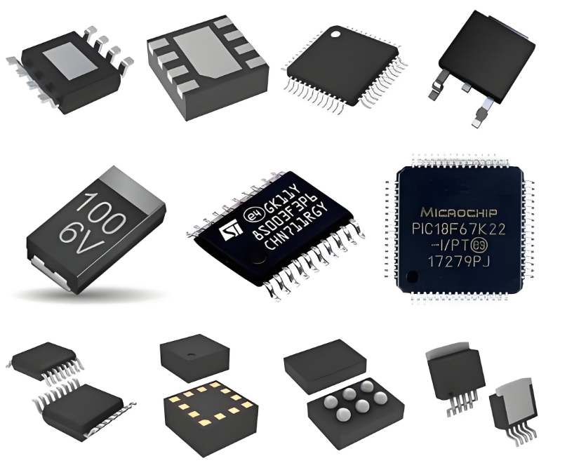
Lattice ICE40LP8K-CM121: A Comprehensive Overview of its Architecture and Applications
The Lattice ICE40LP family represents a cornerstone of low-power, cost-sensitive programmable logic solutions. Among its members, the ICE40LP8K-CM121 stands out as a particularly versatile FPGA, engineered to deliver a balance of performance, power efficiency, and a compact footprint. This article provides a detailed examination of its internal architecture and explores its diverse application space.
Architectural Deep Dive
The architecture of the ICE40LP8K-CM121 is a masterclass in optimized design for low-power operation. Its core components are meticulously arranged to maximize functionality while minimizing silicon area and power consumption.
At the heart of the device lies a sea of Programmable Logic Blocks (PLBs). Each PLB contains essential elements like a 4-input Look-Up Table (LUT) that can be configured as a distributed RAM or a shift register, a flip-flop, and carry logic for efficient arithmetic operations. This granular structure allows designers to implement highly customized digital circuits with high efficiency.
A critical feature enabling its low-power reputation is the programmable I/O bank structure. The device supports a wide range of voltage standards (LVCMOS, LVTTL, PCI, etc.), allowing for seamless interfacing with other components in a system. More importantly, its ultra-low power sleep mode is a key differentiator. The FPGA can enter a state where static power consumption drops to mere microamps, making it ideal for battery-powered applications that spend significant time in a standby state.
For moving data on and off the chip, the ICE40LP8K-CM121 is equipped with hardened intellectual property (IP) blocks. It features high-speed I/O interfaces capable of supporting SPI and I²C, which are ubiquitous for communicating with sensors and peripherals. This eliminates the need to use precious general-purpose logic for these common functions, saving power and resources.
Furthermore, the device includes embedded block RAM (EBR). These 4k-bit blocks provide efficient on-chip memory storage for data buffering, FIFOs, or serving as small lookup tables, enhancing the overall performance of designs by reducing external memory accesses.
Diverse Application Domains
The unique blend of low power, small size, and sufficient logic capacity (8K LUTs) opens the door to a multitude of applications.

Portable and Battery-Powered Electronics: This is the primary domain for the ICE40LP8K. It is perfectly suited for sensor aggregation and bridging in devices like smartwatches, fitness trackers, and handheld medical instruments. It can power-manage sensors, pre-process data (e.g., filtering, averaging), and bridge different communication protocols (e.g., translating between I²C and SPI) before sending clean data to the main application processor, drastically reducing the system's overall power budget.
Consumer Electronics: In smart home devices, drones, and advanced remote controls, the ICE40LP8K can act as a hardware co-processor for real-time control and interfacing. It manages motor controls, button debouncing, LED dimming patterns, and touch sensor inputs, offloading these time-critical tasks from the main CPU.
Industrial Control and IoT: For the Internet of Things (IoT), the FPGA serves as a flexible hardware management unit. It can implement glue logic, real-time state machines for system control, and secure boot functions. Its resilience and deterministic operation make it valuable in industrial environments for tasks like PLC I/O expansion and motor drive control.
System Management: A very common use case is as a "Power Management Controller" on a larger board. It can sequence the power-up and power-down of various ASICs and processors, monitor system temperatures and voltages, and manage fan speeds, ensuring a stable and reliable boot process and operational environment.
The Lattice ICE40LP8K-CM121 is a quintessential low-power FPGA that excels in bridging, interfacing, and control tasks. Its highly optimized architecture, featuring efficient programmable logic, embedded memory, and hardened IP for common interfaces, is specifically designed to minimize power consumption without sacrificing critical functionality. Its value proposition is strongest in applications where extending battery life, managing multiple peripherals, and implementing real-time control are paramount, making it an indispensable component in modern portable and embedded system design.
Keywords:
1. Low-Power FPGA
2. Programmable Logic Architecture
3. Sensor Aggregation
4. Hardware Management Unit
5. Battery-Powered Applications
